
If you have ever tried to remove a large area of the laminated copper surface from a sheet of printed circuit board (PCB) you will know how tenacious the bonding is between the thin layer of copper and the fibre glass substrate.
This strength can be used to advantage in the fabrication of structures that emulate sheet metal but without the need for folding or welding to bond them together. All that is needed is single or double sided PCB sheet, an ability to cut to a size, flux paste, soldering iron and asbestos fingers. Using single or double sided PCB allows flexibility on whether joints are single sided or double sided. The resulting structure will be amazingly strong.
Process
1 Design your structure as if it was being made from sheet metal. Decide if single or double sided joints are needed to replace the folds on the sheet metal equivalent.
2 Copper clad board can be bought from RS, CPC etc but I would recommend a visit to your local PCB manufacturer and scrounge some off-cuts sufficient for your project needs. He will have pallets of scrap pieces going off to be recycled. Off-cuts are usually clean copper rather than tinned and will be in various industry standard thicknesses and these days are often multilayer making the material even tougher against flexing. I use 1.6mm (1/16″) for my projects but it is useful to have other thicknesses to hand such as 1/32” and even 1/8”.
3 Cut the PCB (either double or single sided) to the net shapes needed. These will all be flat pieces and the solder joints you will be making will replace the conventional sheet metal folds. The positive aspect of this technique is that you can get the finished article to fit exactly what you are trying to achieve. No allowances are needed for fold material etc and all holes for fittings can be made on the appropriate flat PCB sheet while still flat.
The Gabro 2M2 or similar notching guillotine is a real asset for cutting to size. The notched strips of PCB created by the guillotine blade are useful scrap to employ for ribbing.
4 Scrub clean the border surfaces to be soldered with an abrasive block or fine steel wool and then smear with flux paste. My preference is to use traditional Fluxite.
5 Tack solder the components together. I admit to preferring lead based traditional 60/40 Multicore for this work. Note that differential heat expansion will tend to ‘pull’ right angle surfaces over, so use a 123 block or similar to maintain the angle. Once tacked in place fully flow the seam joints using a large, high temperature iron bit with a copious solder feed. Keep pressure on right angle components even after tacking to avoid thermal pull over. You will soon pick up the knack for getting a smooth filet that is almost like a weld in appearance.
6 If fixings are needed (i.e. for removable lids etc) then sweat an appropriate brass nut to the copper surface on the body to pick up on matching fastener holes. Likewise mounting holes can have larger nuts soldered in place in the manner of a sheet metal hank bush. When soldering nuts in place, hold them in position using steel screws smeared with a little MS4 silicon grease or similar so the screw doesn’t get soldered into the nut.
7 Clean the finished seams with thinners or similar to remove the baked flux residues. If you want a bright finish, wash the completed joints with Swarfega or similar hand cleaner.
8 Paint and finish as required. Standard aerosol primer and finishing coats take well to the fibre glass and copper.
Other PCB Comments
A If you ask the PCB maker he will quite often be prepared to tin the copper for you but some financial persuasion might be needed. This makes the look of the finished project better in that you don’t have the distraction of a tinned solder seam at the edges with unfinished copper everywhere else.
The alternative is to hand tin. This is much easier than it sounds. Take the flat components of your project and scrub clean. Smear the clean copper all over with flux paste. Using a wide chisel bit soldering iron, simply run the iron up and down the copper in overlapping runs while feeding solder. Don’t overfeed the solder or you will get ridges in the finish. It will look horrible until you wash off the flux.
Use thinners or Acetone first of all to remove the baked flux residues and then use Swarfega or similar hand cleaner to give the final polish. Once you get skilled at this process, the witness marks of your soldering strips will not be obvious after cleaning. If it looks a bit rough then use some SoderWick to such off the excess.
Note this same hand tinning process can be used on home etched printed circuit board tracking. When applying solder in this way on thin tracks and lands, reduce the size of the soldering iron bit and keep the soldering iron movement fast so as not to dwell and destroy the bond between the copper and fibre glass substrate.
B If the project is electrical in nature, note that the copper surface can be easily isolated into electrical pads and conductors if required. The copper surface will, with design planning, be electrically conductive all the way through the fabrication so a negative supply return is automatically provided and the copper soldered to at any point. This is a big advantage over metal construction where there is a need to have bolted earth tags. Through links using 22SWG TCW or rivets can be used where conductivity between surfaces is not achieved in the soldered construction. I used this technique on the Laser Centring tool battery cover for my Myford VMB milling machine.
Cable forms can be held in place with a simple saddle of 22SWG or similar bridging the cable. Put some insulating sleeving on the saddle wire to stop the hot bridge wire from melting into the cable being held when soldering.
C For those with engraving facilities you can engrave the front panels of projects by milling off the copper surface to reveal the contrasting bare fibre glass.
D Items made with this PCB technique will be much lighter than a metal equivalent. This might be important for instance in airborne payloads. A further advantage is that the seams created in the described technique will be watertight.
E Not totally related but useful to know is a technique for removing copper from PCB. With the common availability of surface mount devices (SMD) it is convenient to cut a prototype PCB as a series of lines and rectangles onto copper clad board with a scalpel or similar and to remove the intervening strips to isolate the conductors. When trying to lift the copper, if the board has un-tinned copper, the copper frustratingly tends to tear towards any nicks and come away in small pieces. If the section to be removed is tinned beforehand with the flux and iron technique it adds strength to the copper.
After tinning, lift one corner of the section to be removed and gripping with long nosed pliers, pull away from the PCB backing while slowing running the soldering iron ahead of the moving lifting point. The heat acts to degrade the epoxy bond between copper and fibreglass and the whole section will come away in one piece. Large areas can be stripped in this way but for ease of process, the strip sections should not exceed 10mm wide.
Once the wanted conductors only are left on the prototype board, there will be burrs on the edges from the scalpel action. These should be scrub removed and then the remaining wanted conductors can be cleaned, fluxed and tinned as described earlier.
F Definitely totally unrelated – do you have a persistent crack in a wall that no matter how many times you fill it and paint over it just comes back ? The chances are that there is some differential movement between the two sides of the crack. Cut some strips of PCB and brutally hammer them edge ways into the crack at regular intervals along the crack line. Make sure they are sub surface and then fill the crack and paint over. The PCB stops the differential movement between the two sides and the crack will not re-appear.
Constructed Example
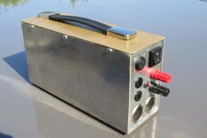
Photo 1 shows a universal 12V battery box completely fabricated using this technique. The box was made from 1.6mm single and double sided PCB.
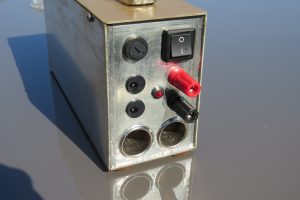
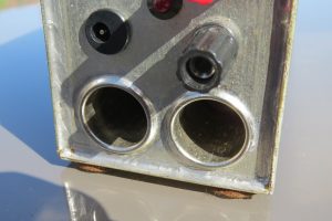
The front panel is shown in Photo 2 and the zoomed image in Photo 3 shows how the 12V car socket outlets have been re-flowed directly onto the panel copper.
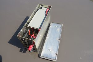
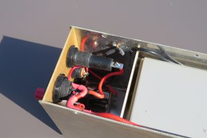
Photo 4 shows the lid removed and the wiring is shown in Photo 5. Note the wiring held in place by wire saddles.
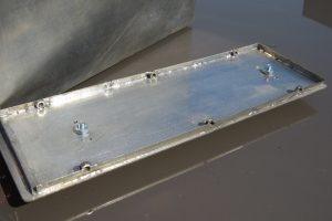
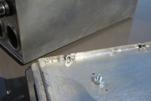
The lid is shown in Photo 6 and has a nickel silver rib soldered in place onto which the lid retaining nuts are soldered as shown in Photo 7. PCB strips could have been used rather than nickel silver.
Conclusion
The technique is clearly never going to produce items with similar strength to a steel equivalent. However I think you will be surprised just how robust the finished items will be and how easy it is to quickly knock up custom boxes and structures using this method.