
One way of doing it
Many of the Arduino related modules have their own PCB with the relevant semiconductors on board. This creates a chicken and egg situation when creating the library parts to match. Remember that some of these modules are slightly different in their physical appearance dependent on supplier. The manufacturers do not always have a library file to offer or a detailed dimensioned drawing. The manufacturers also do not seem to profile the PCB accurately. The SSD1306 is a good example where the mounting holes are in slightly different places dependent on source. One particularly tricky one is the DS3231 RTC module. This has two sets of matching pads and three mounting holes and as far as my searching goes, there are no detailed drawings available. My process on the DS3231 was to scan the board and use the Fusion ‘first dimension’ scaling rule. Here are the steps.
First step is to make sure you have ‘Scale Entire Sketch to First Dimension’ ticked in Fusion Prefs/General/Design.
If the board has one side unpopulated with components this is ideal to get an image of it. You can use a mobile phone or similar but there will be distortions in the resulting image due to lens geometry. My preferred method is to place the flat side of the board on my office scanner, scan and save the image as a jpg. Try to scan it so there is little or no rotation off square. The easiest way is to locate the board up to the platen edge. The DS3231 does not have a flat side and I resorted to removing the battery holder to allow a flat scan…. perfectionist did I hear you say ? ….
Import the resulting jpg image as a Canvas into Fusion and set up the workspace to be in Imperial units. Use the image as a Canvas background to trace and locate the key aspects of pad locations and mounting holes etc. Try to be as accurate as you possibly can with your tracing. The important aspect of the traced features is their X and Y location. Hole sizes are not critical at this stage just the location of the hole.
The outer perimeter of the board is less critical on accuracy.
Do not dimension anything at this stage so your traced image should all be in blue lines.
Once you have all the key aspects traced, measure a key dimension on the actual board and mimic this same dimension on your sketch and dimension it to match the actual measured value. This is a critical step as any error in your physical measurement will magnify or shrink your resulting sketch. The sketch should now have expanded to match your measurement and can now be used to accurately measure the remaining geometry locations.
Continue with the sketch dimensioning tool to document the X and Y positions of the geometry of interest. Do not dimension to the outline as it won’t be accurate. Instead think about where you want the placement zero to be in Fusion Electronics and then dimension to this. Components such as 0.1”SIL connectors make a useful cross check that things are progressing well. SILs also make good locations for X0Y0 using a point midway along the SIL pad array.
Once you have a sketch showing all the key locations you can proceed in FE to create the symbol and the footprint. Use the Properties ‘right click’ on pads to accurately locate them in relation to your sketch X0Y0 location. Use pads as mounting hole location markers.
When all the locations are entered, draw a nominal outline as the silk screen image.
With the footprint complete, use the ‘three dot’ route to creating the 3D model. Fusion modelling workspace will open with the faint outline of the footprint you have just created and you can then build the 3D model to match the geometry and holes etc.
If you attempt to create the 3D model first without the matching sketch of the geometry you are going to have fun trying to make the footprint and the 3D model match each other.
Once you are happy with the footprint and the 3D model don’t forget to use the joint command to locate a ‘hole to a hole’ to lock the footprint and the 3D model.
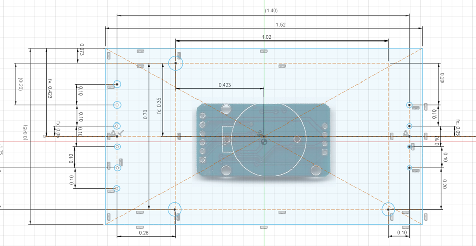
It sounds complicated but it works…. once you have the routine clear in your head. Below is the Canvas import of the DS3231 and the resulting sketch created after the Canvas trace had been scaled up. Engineers creating the Arduino modules seem to lack a certain discipline. The electronic parts all get nicely placed (hopefully on 50 thou related positions) and then they seem to arbitrarily position the mounting holes where they can find some remaining space to fit them in.
These additional notes have been added to my Fusion Electronic library waffle document that you can download on the link below.
Links to similar or related post are listed below : –