
Implications of milling tools and FlatCAM settings
I have spent many hours CNC milling circuit boards and I have documented my process elsewhere on this blog. The workflow is to first design the board in Fusion Electrical (or any similar CAD package) and export the manufacturing package as Gerber files for the copper artwork and an Excellon file for the drilling information. The manufacturing files can be imported into FlatCAM to convert them to CNC files for milling operations. This is all documented in my various ramblings. Double and single sided board are both accomodated by the FlatCAM software (you just need to get your head around manipulating the artworks).
I have been reasonably happy with the results that I achieve but as ever I tend not to rest with a process which has some niggles. As a result I keep searching for a breakthrough lightbulb moment or at least an interative advancement to make the results more repeatable/easier etc.
The first irritation was the cost of the milling tools I was using. I bought these in from Think and Tinker in the US and they cost around USD20 each for a 5 thou end mill. One careless twitch and your bank account takes a hit.
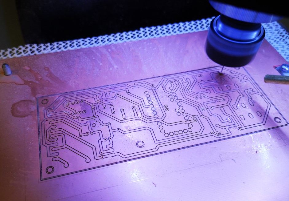
Let’s take a step back and refresh. The FlatCAM process produces a file that moves the cutter around a copper clad board to leave isolated representations of the copper trackwork. The gap between the wanted trackwork and the rest of the unwanted copper is defined by the width of the milling cutter. FlatCAM allows you to widen the isolating gap by taking additional milling paths side by side to each other with a defined overlap. With a 5 thou cutter I used to take two parallel cuts with a 10% overlap so the resulting gap was 9.5thou. This is a pretty narrow gap. The second time round cut does tend to raise burrs/slivers of copper and these can easily cause a bridge between the wanted and unwanted trackwork.
I make this more difficult for myself as I prefer to tin the copper after milling. (Scrub the copper clean, daub with flux and then deftly swish a soldering iron across the copper). The end result is good but the road to it is fraught. Before tinning, the board needs to be checked for milling shorts and all milling debris removed and scrubbed clean. After the tinning process there will be a number of self induced solder bridging shorts which also have to be cleared. A quick post tinning run round the board with SolderWick is a fast track route to remove these. The process works and the tinned end result looks much better than bare copper.
The first area of my current investigation was the milling tools. Could a larger diameter milling tool be sourced at a price advantage to the US parts and how much larger diameter would be practical to give acceptable artworks. The solution came from APT Tooling who are one of my regular suppliers of tooling. They provide a range of micro milling tools starting from 0.3mm (11.8 thou) and upwards. A single pass at this size would achieve the same isolating gap as the two passes with overlap with the 5 thou parts. Potentially a single path would reduce the swarf debris. APT offer two versions of the micromills with different hardnesses.
My PCB artworks are not high density and with my eyesight constraints I tend to stick with through hole components whenever possible and 40thou trackwork. I ordered in 0.3mm and 0.4mm milling bits (55 HRC versions) and ran the FlatCAM simulations of the 0.4mm isolation routing. The 0.4mm (15.7 thou) had the distinct advantage of creating a wider isolation gap while still allowing inter pin gaps to be cut. Adding a second cut with the same 10% overlap created a very acceptable artwork with a generous isolation gap. FlatCAM is nice in that providing the first pass can cut 100% of the isolation artwork, the second cut automatically truncates cutting gaps that would not be compatible with the artwork and damage the geometry. Here are some FlatCAM simulations
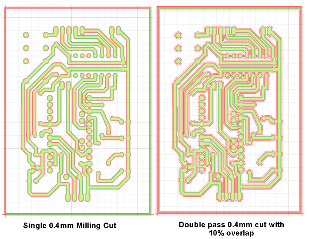
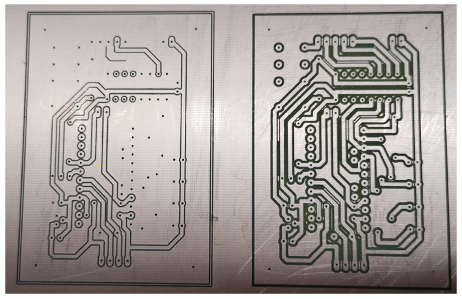
Here are the actual results of an artwork cut as a single 0.4mm cut and as a double cut with 10% overlap. (I terminated the single cut as the resulting partial artwork was enough to make a decision on). Notice that the double cut does leave mini floating islands between wanted trackwork as shown in the simulations. These can be easily removed with a hot soldering iron.
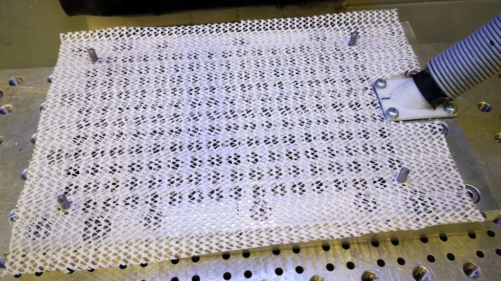
Whenever I get a new supply of PCB material I strip peel a small section and measure the thickness of the copper and the overall thickness of the board. Currently I am using RS single sided board (RS#219-2123) and this measures 2 thou copper and 60 thou overall. With this material I am running a 4 thou depth with a feed rate of 10″ per minute. I run all PCB operations on my Tormach PCNC440 with my home made vacuum plate.
Conclusion – for my level of artwork density I now believe I can get acceptable results using a 0.4mm cutter in either a single cut or overlapping double cut process. The APT 0.4mm tools are much lower cost than the US sourced parts and being larger diameter will hopefully be more robust. To date I have only tried their 55RHC versions. Note I always run both the milling cuts and drilling routines with spray coolant from a Fogbuster with my normal spray coolant (QualiChem Xtreme Cut 250C) . This has the advantage that the fluid enters the cuts and shows as a clear black line when the cut depth is correct or at least deep enough to go through the copper.
If anyone wants more information about my process, please get in touch.
Links to similar or related post are listed below : –
- Further experiments milling PCBs
- Editing irregular PCB shapes in FlatCam
- Vacuum table update for PCB milling
- Update on CNC milling printed circuit boards on a homemade vacuum table
- Experiences and understanding FlatCAM PCB milling program
- Clamping of printed circuit boards while milling tracks follow up
- A Mini Vacuum Clamping Table for PCB Engraving
- Stretching FlatCam and PCB milling on Tormach PCNC440
- Milling Circuit Boards Update
- FlatCAM Update and experimental copper cutting